- Rigid PCB[6]
- Multilayer PCB[6]
- Other PCB & PCBA[6]
- FPC[6]
- Double-Sided PCB[1]
- Other Electronic Components[1]
- Contact Person : Ms. Zeng Bluesky
- Company Name : Shenzhen Xindaxing Electric Technology Co., Ltd.
- Tel : 86-0755-29621535
- Fax : 86-0755-29094381
- Address : Guangdong,Shenzhen,818#,Zhaofengxiang Building,Liye Road,Songgang Town, Bao'an District,Shenzhen
- Country/Region : China
- Zip : 518105
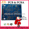
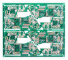
8 layers pcb/ BGA PCB


Related Product Searches:8 layers pcb/ BGA PCB,High Quality,8 layers bga pcb, bga pcb,8 layers pcb/ BGA PCB
| Welcome to XinDaxing Electric Technology Co., Ltd 8-layers pcb/ BGA PCB We can prvide a package of service: 1. PCB layout, PCB design; 2: Make high difficulty PCB(1 to 38 layers) 3: Provide all Electronic components; 4: PCB assembly; 5: Write programs for clients; 6: PCBA/finished product Test. etc… |
1.Specification for PCB Manufacture:
Item | Specification |
Numbr of Layer | 1-38Layers |
Material | FR-4,FR2.Taconic,Rogers, CEM-1 CEM-3,ceramic , crockery |
Metal-backed Laminate | |
Remarks | High Tg CCL Is Availabe(Tg>=170ºC) |
Finish Board Thickness | 0.2mm-6.00 mm(8mil-126mil) |
Minimun Core Thickness | 0.075mm(3mil) |
Copper Thickness | 1/2 oz min;12 oz max |
Min.Trace Width & Line Spacing | 0.075mm/0.1mm(3mil/4mil) |
Min.Hole Diameter for CNC Driling | 0.1mm(4mil) |
Min.Hole Diameter for punching | 0.9mm(35mil) |
Biggest panel size | 610mm*508mm |
Hole Positon | +/-0.075mm(3mil) CNC Driling |
Conductor Width(W) | +/-0.05mm(2mil)or |
+/-20% of original artwork | |
Hole Diameter(H) | PTH L:+/-0.075mm(3mil) |
Non-PTH L:+/-0.05mm(2mil) | |
Outline Tolerance | +/-0.125mm(5mil) CNC Routing |
+/-0.15mm(6mil) by Punching | |
Warp & Twist | 0.70% |
Insulation Resistance | 10Kohm-20Mohm |
Conductivity | <50ohm |
Test Voltage | 10-300V |
Panel Size | 110×100mm(min) |
660×600mm(max) | |
Layer-layer misregistration | 4 layers:0.15mm(6mil)max |
6 layers:0.25mm(10mil)max | |
Min.spacing between hole edge to circuity pqttern of an inner layer | 0.25mm(10mil) |
Min.spacing between board oulineto circuitry pattern of an inner layer | 0.25mm(10mil) |
Board thickness tolerance | 4 layers:+/-0.13mm(5mil) |
6 layers:+/-0.15mm(6mil) | |
Impedance Control | +/-10% |
Different Impendance | +-/10% |
2.Our Major Customers:
3.View of XinDaXing:
8 layers pcb/ BGA PCB