- Rigid PCB[6]
- Multilayer PCB[6]
- Other PCB & PCBA[6]
- FPC[6]
- Double-Sided PCB[1]
- Other Electronic Components[1]
- Contact Person : Ms. Zeng Bluesky
- Company Name : Shenzhen Xindaxing Electric Technology Co., Ltd.
- Tel : 86-0755-29621535
- Fax : 86-0755-29094381
- Address : Guangdong,Shenzhen,818#,Zhaofengxiang Building,Liye Road,Songgang Town, Bao'an District,Shenzhen
- Country/Region : China
- Zip : 518105
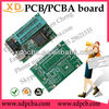
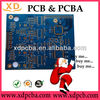
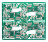
Two Layers PCB With Immersion Gold treatment


Related Product Searches:Two Layers PCB With Immersion Gold treatment,High Quality,immersion gold pcb, 2 layers pcb board,immersion gold finish pcb board
Welcome to XinDaxing immersion gold finish pcb board
Shenzhen Xindaxing Electric Technology Co., Ltd.
(Xing Da Electric Technology Co.,Ltd),which has been specializing in PCB/PCBA and Electronic components for many years.
We can prvide a package of service:
1. PCB layout, PCB design; 2: Make high difficulty PCB(1 to 38 layers) 3: Provide all Electronic components; 4: PCB assembly; 5: Write programs for clients; 6: PCBA/finished product Test. etc…1.Specification for PCB Manufacture:
Item | Specification |
Numbr of Layer | 1-38Layers |
Material | FR-4,FR2.Taconic,Rogers, CEM-1 CEM-3,ceramic , crockery |
Metal-backed Laminate | |
Remarks | High Tg CCL Is Availabe(Tg>=170ºC) |
Finish Board Thickness | 0.2mm-6.00 mm(8mil-126mil) |
Minimun Core Thickness | 0.075mm(3mil) |
Copper Thickness | 1/2 oz min;12 oz max |
Min.Trace Width & Line Spacing | 0.075mm/0.1mm(3mil/4mil) |
Min.Hole Diameter for CNC Driling | 0.1mm(4mil) |
Min.Hole Diameter for punching | 0.9mm(35mil) |
Biggest panel size | 610mm*508mm |
Hole Positon | +/-0.075mm(3mil) CNC Driling |
Conductor Width(W) | +/-0.05mm(2mil)or |
+/-20% of original artwork | |
Hole Diameter(H) | PTH L:+/-0.075mm(3mil) |
Non-PTH L:+/-0.05mm(2mil) | |
Outline Tolerance | +/-0.125mm(5mil) CNC Routing |
+/-0.15mm(6mil) by Punching | |
Warp & Twist | 0.70% |
Insulation Resistance | 10Kohm-20Mohm |
Conductivity | <50ohm |
Test Voltage | 10-300V |
Panel Size | 110×100mm(min) |
660×600mm(max) | |
Layer-layer misregistration | 4 layers:0.15mm(6mil)max |
6 layers:0.25mm(10mil)max | |
Min.spacing between hole edge to circuity pqttern of an inner layer | 0.25mm(10mil) |
Min.spacing between board oulineto circuitry pattern of an inner layer | 0.25mm(10mil) |
Board thickness tolerance | 4 layers:+/-0.13mm(5mil) |
6 layers:+/-0.15mm(6mil) | |
Impedance Control | +/-10% |
Different Impendance | +-/10% |
2. Details of tech:
PCB/ PCBA Technic
1).Professional surface mounting and through hole soldering technology;
2).Various sizes,like 1206,0805,0603 components SMT technology;
3).ICT(In Circuit Test),FCT(Functional Circuit Test) technology;
4).Nitrogen gas reflow soldering technology for SMT;
5).High standard SMT&Solder Assembly line;
6).High density interconnected board placement technology capacity.
PCB/ PCBA Quote requirement
1).The detailed files(Gerber file/ PADS/ AutoCAD/ Protell/ Power PCB/ DWG/ schematic etc and BOM);
2).Clear pictures of PCBA or samples for us;
3.View of XinDaXing:
1) PCBA Factory
2) PCB factory
3) PCB/ PCBA Test corner
4. Why us?
Quality
Our UL/Rohs standards garantee our quality from start to finish. Whether it's a simple custom product or a complex production run, XingDa will adhere to the highest quality standards.
Capabilities
XingDa offers the latest and best capabilities and qualifications ensuring highest quality in each piece of product we produce.
Experience
We have been specializing in PCB and PCBA industry for many years. Our management and engineering team possess over 10years combined PCB and PCBA experience, so does our sourcing team.
Protecting your interests
Protecting your Intellectual Property comes first! All your files/ information regarding design of your products will only be used for your projects, will never be leaked out.
Price and leadtime
We will offer the best price and shortest leadtime for your PCB and PCBA since we have professional engineering department, sourcing department and producing department etc.
5. Delivery and Payment:
1. By DHL, UPS, FedEx, TNT etc.
2. By EMS (Usually for Russia Clients), price is high.
3. By sea for mass quantity according to customer's requirement.
4. By customer's Forwarder
5. payment prefer -- T/T, Western Union ( HSBC )
If any need or questions, please feel free to contact me any time. You can send me email or inquiry via Alibaba. Thank you.
Two Layers PCB With Immersion Gold treatment